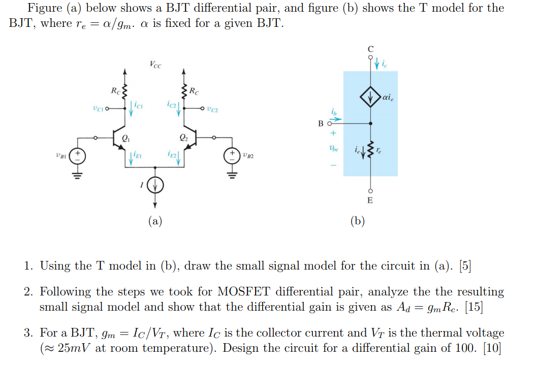
Solved Figure (a) below shows a BJT differential pair, and
BJT differential pair Asked 6 years, 10 months ago Modified 6 years, 10 months ago Viewed 635 times 0 I am struck . Currently working in sedra Smith , I stumbled across this question in BJT differential pairs . now I am confused as to how to determine which transistor will conduct and which will not . Can anyone help me please transistors Share

PPT Chapter 8 Differential and Multistage Amplifiers PowerPoint Presentation ID6728878
A single BJT differential pair is shown below. For RL1 and RL2 =1 k , calculate IBIAS to set VO1 and VO2 at a level that will give the maximum output swing. Assume VCEsat =0.2 V and VBE = 0.7 V. With your value of IBIAS calculate the differential mode gain Adm = vout/vin and the common mode gain Acm=vout/vin. What is the CMRR? FIGURE 1.
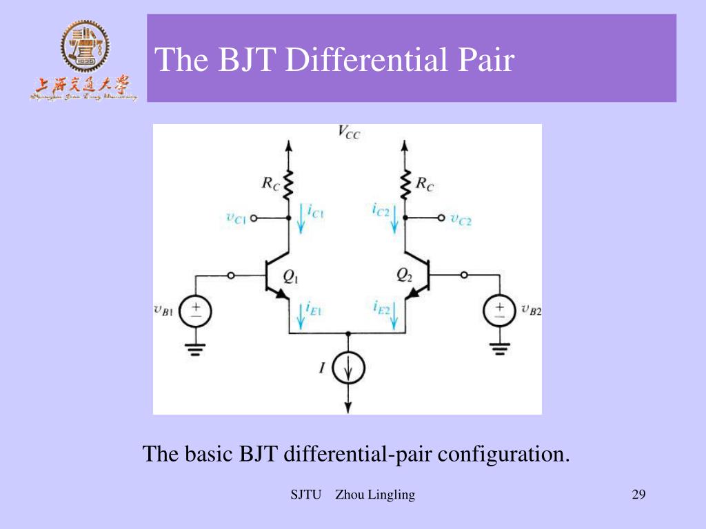
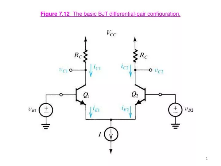
PPT Figure 7.12 The basic BJT differentialpair configuration. PowerPoint Presentation ID
MOSFET Differential Amplifiers Reading: Chapter 10.3‐10.6 Prof. Common‐Mode (CM) Response • Similarly to its BJT counterpart, a MOSFET differential pair produces zero differential output = V V = V − X Y DD R I SS D 2 2 Prof. Equilibrium Overdrive Voltage

PPT Semiconductor Physics & Bipolar Junction Transistor (BJT) PowerPoint Presentation ID6658125
load and parasitic capacitances. Saturation in ECL is avoided by using the BJT differential pair as a current switch.5 The BJT differential pair was studied in Chapter 9, and we urge the reader to review the introduction given in Section 9.2 before proceeding with the study of ECL. 15.4.1 The Basic Principle
PPT Chapter 5 Differential and Multistage Amplifier PowerPoint Presentation ID502585
The BJT differential AMP with an active. Many IC amplifiers use BJT loads in resistance, R . C. BJT load resistor is usually connected as a constant-current source with a very high resistance load (output resistance of the current source) Higher load resistance, higher output gain.

Differential Amplifier Circuit Tutorial Using Bjt And Opamp Riset
The objective of this activity is to investigate a simple differential amplifier using NPN transistors. First, we need to make a few notes on hardware limitation issues. The waveform generator in the ADALM2000 system has a high output bandwidth and with that high bandwidth comes wideband noise.
PPT Figure 7.12 The basic BJT differentialpair configuration. PowerPoint Presentation ID
The differential amplifier can be implemented with BJTs or MOSFETs. A differential amplifier multiplies the voltage difference between two inputs (Vin+ - Vin-) by some constant factor Ad, the differential gain. It may have either one output or a pair of outputs where the signal of interest is the voltage difference between the two outputs.
PPT Semiconductor Physics & Bipolar Junction Transistor (BJT) PowerPoint Presentation ID6658125
Lecture 1 Lecture 24 OUTLINE MOSFET Differential Amplifiers Reading: Chapter 10.3‐10.6 Common‐Mode (CM) Response • Similarly to its BJT counterpart, a MOSFET differential pair produces zero differential output as V changes. V X Y V = = V DD R − SS 2 Equilibrium Overdrive Voltage
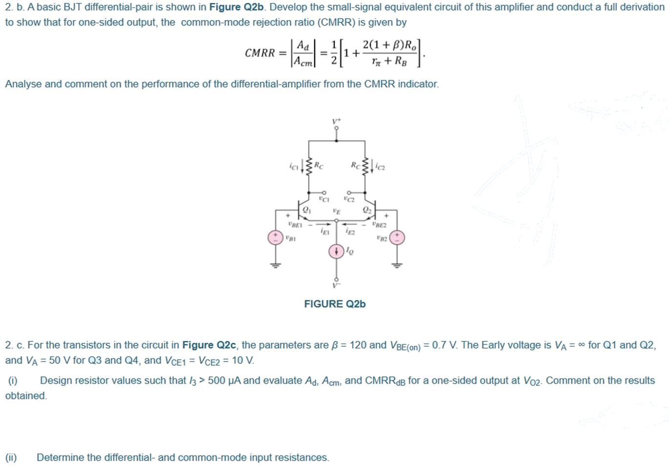
(Get Answer) 2. B. A Basic BJT DifferentialPair Is Shown In Figure Q2b.... Transtutors
Institute for Information Sciences Home | I2S | Institute for.. 3:; :
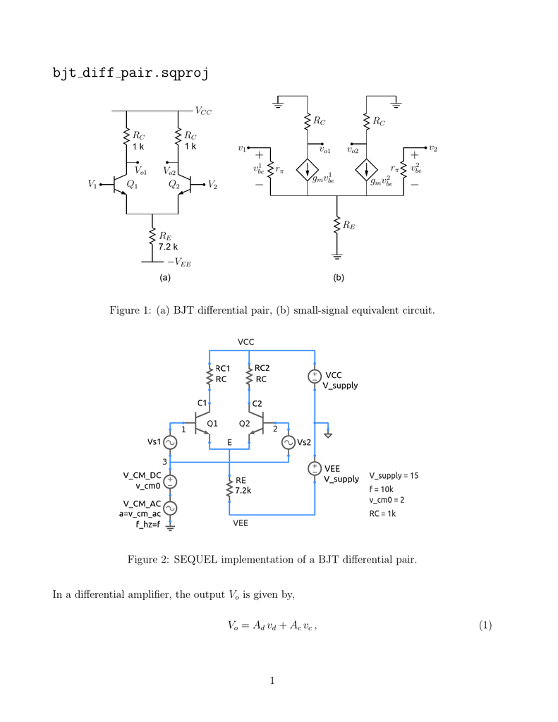
bjt_diff_pair.sqproj (BJT differential pair (without RE))
BJT Differential Amplifiers (cont'd) Cascode differential amplifiers Common‐mode rejection Differential pair with active load Reading: Chapter 10.4‐10.6.1 Effect of Finite Tail Impedance • If the tail current source is not ideal, then when an input common‐mode voltage is applied, the currents in Q 1 and Q 2
In a differential pair BJT amplifier, the individual gain of the transistors should be equal
BJT Differential Pairs Now lets consider the case where each input of the differential pair consists of an identical DC bias term V B, and also an AC small-signal component (i.e., v 1(t) and v 2(t)) CC As a result, the open-circuit output voltages will likewise have a DC and small-signal component. V V EE R C I v O2 ()t v O1
The Differential Amplifier BJT Differential Pair
In this video, the design and working of BJT- differential amplifier is explained. By watching this video, you will learn the following topics:0:00 Introduct.
PPT Figure 7.12 The basic BJT differentialpair configuration. PowerPoint Presentation ID
• BJT Differential Amplifiers (cont'd) - Cascode differential amplifiers - Common‐mode rejection - Differential pair with active load EE105Spring 2008 Lecture23, Slide 1Prof.Wu, UC Berkeley • Reading: Chapter 10.4‐10.6.1 Cascode Differential Pair Half circuit for ac analysis.
PPT Figure 7.12 The basic BJT differentialpair configuration. PowerPoint Presentation ID
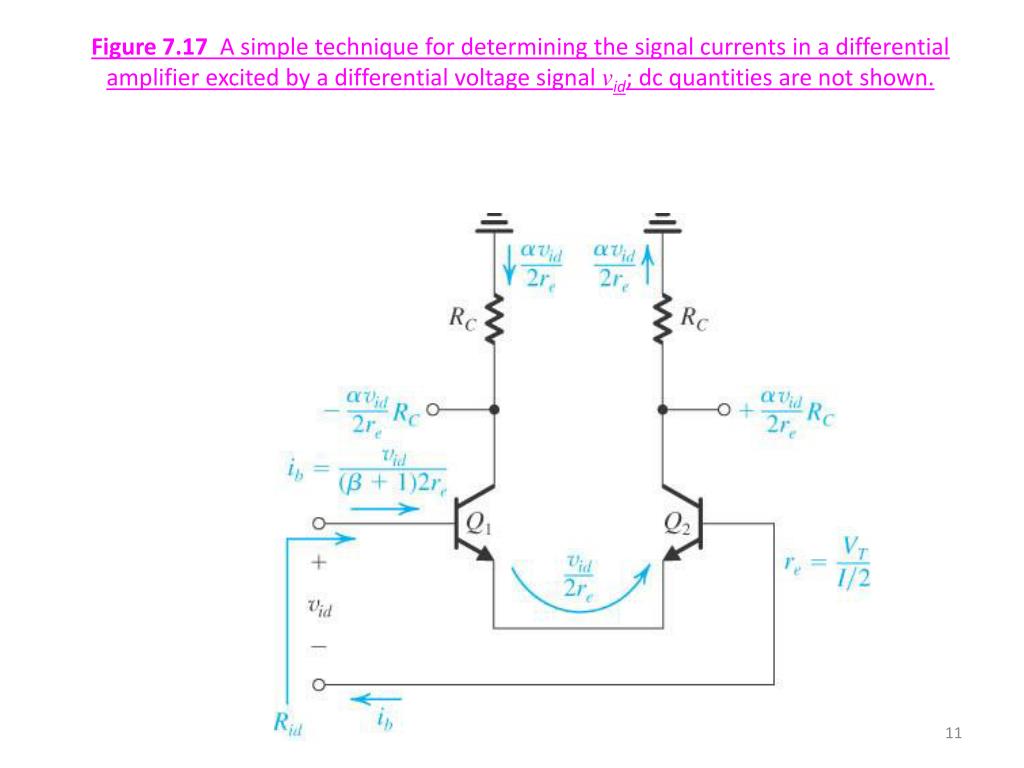
5/6/2011 section 7_3 The BJT Differential Pair 1/1 Jim Stiles The Univ. of Kansas Dept. of EECS 7.3 The BJT Differential Pair Reading Assignment: pp. 704-720 In addition to common-emitter, common-collector (i.e., the emitter follower), and common-base amplifiers, a fourth important and "classic" BJT amplifier stage is the differential pair.
PPT Chapter 6 Differential and Multistage Amplifiers PowerPoint Presentation ID1199584
It refers to the gain of the transistor, collector current divided by base current. You can consider the 1 mA evenly distributed as a first order approximation. In reality, this only happens right at the cusp where the differential pair is in balance.
PPT Figure 7.12 The basic BJT differentialpair configuration. PowerPoint Presentation ID
BJT Differential Pair Osc A BJT version of the oscillator has limited voltage swing determined by the differential pair non-linearity. We can increase the voltage swing by emitter degeneration. A more popular alternative is to provide feedback capacitors. The negative conductance is decreased by the feedback factor.